AuTeSe

AuTeSe

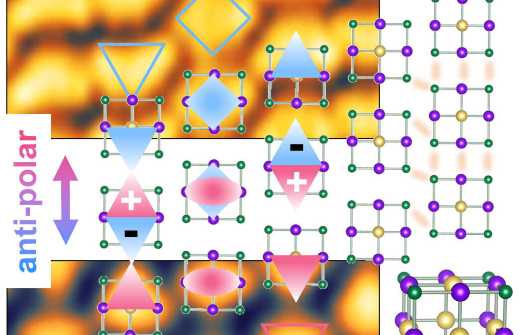
Fig.1 Intercube Te-Te quasibonds and two interweaved charge orders in the ATS superatomic crystal

.

Physical review X

Interweaving Polar Charge Orders in a Layered Metallic Super-atomic Crysta

A superatom is any cluster of atoms that collectively exhibits some properties of single atoms. When arranged into crystals through the noncovalent bonds, they can be readily assembled into nanostructures, because the reduced cohesive energy of the noncovalent bonds makes it easier to cleave the material. It is not yet clear whether such weakened energetic interaction is accompanied by a suppressed electronic interaction among the superatoms. To that end, we explore exotic electronic structures on the surface of one superatomic crystal and find strong electron-electron interactions do occur. We also find that two exotic charge orders emerge.

Recently, researchers synthesized a cubic superatom, Au6Te12Se8 (ATS), and assembled it into a 3D crystal with metallicity and superconductivity.[9] In our experiments, we observe two charge orders on the ATS surface. One is a charge density wave that forms across repeating columns of ATS cubes. The other is a polar metallic state that arises between the columns. The polar metallic states are of particular interest, suggesting the ATS surface is an antipolar metal—a type of exotic metal where metallicity and orderly, antiparallel-oriented electric dipoles coexist. The discovery of this antipoloar metal goes one step further toward the realization of multifunctional devices, which could, in principle, perform simultaneous electrical, magnetic, and optical functions. However, we have not yet examined ATS’s ferroelectricity, which is needed for electrical control of its electrical polarization.

This ATS crystal is, to the best of our knowledge, the first antipolar metal ever found and possesses the first polar metallic state hosted in superatomic units bound by noncovalent interactions. Thus, the strong electron-electron interactions, found in the 2D superatomic layers, open a category of quantum materials that contains versatile layered nanostructures exhibiting precisely tailorable electronic structures.

REFERENCES

1. Z. Luo, A.W. Castleman, Special and General Superatoms, Accounts of Chemical Research 47 (2014) 2931-2940

2. Superatoms: Electronic and Geometric Effects on Reactivity, (2017)

3. E.A. Doud, A. Voevodin, T.J. Hochuli, A.M. Champsaur, C. Nuckolls, X. Roy, Superatoms in materials science, Nature Reviews Materials 5 (2020) 371-387

4. J. Puru, S. Qiang, Super Atomic Clusters: Design Rules and Potential for Building Blocks of Materials, Chemical Reviews 118 (2018) acs.chemrev.7b00524-

5. Z. Liu, X. Wang, J. Cai, H. Zhu, Room-Temperature Ordered Spin Structures in Cluster-Assembled Single V@Si12 Sheets, The Journal of Physical Chemistry C (2014)

6. E. Meirzadeh, A.M. Evans, M. Rezaee, M. Milich, C.J. Dionne, T.P. Darlington, S.T. Bao, A.K. Bartholomew, T. Handa, D.J. Rizzo, R.A. Wiscons, M. Reza, A. Zangiabadi, N. Fardian-Melamed, A.C. Crowther, P.J. Schuck, D.N. Basov, X. Zhu, A. Giri, P.E. Hopkins, P. Kim, M.L. Steigerwald, J. Yang, C. Nuckolls, X. Roy, A few-layer covalent network of fullerenes, Nature 613 (2023) 71-76

7. Evan, S., O’Brien, M., Tuan, Trin, Rose, L., Kann, Jia, Single-crystal-to-single-crystal intercalation of a low-bandgap superatomic crystal, Nature Chemistry (2017)

8. H. Yang, W. Yu, H. Huang, L. Gell, L. Lehtovaara, S. Malola, H. Hkkinen, N. Zheng, All-thiol-stabilized Ag44 and Au12Ag32 nanoparticles with single-crystal structures, Nature Publishing Group (2013)

9. Guo, J.G., Chen, X., Jia, X.Y. et al. Quasi-two-dimensional superconductivity from dimerization of atomically ordered AuTe2Se4/3 cubes. Nat Commun 8, 871 (2017)

Phase Patterning in 2D Materials

Phase Patterning in 2D Materials

Fig.1 a) The scheme of 2D ReS2 phase transition under STEM. a,b and a + b are the three low index directions of ReS2. e– beam exposure creates a new T phase embedded in the pristine T′ phase. b–d) Atomic structures and electronic structures of T’’ (tetramerization in two directions) phase, T’ (dimerization in one direction) phase, and T (no dimerization) phase from DFT calculation, respectively.

Advanced science

Sub-Nanometer Electron Beam Phase Patterning in 2D Materials

Fig.2 STEM HAADF images of atomic-scale phase transition from pristine T’’ phase into 1D T’ or T phases, via 1D e– beam exposure direction along a, b and a+b crystal directions (scheme on the right), respectively. False color is applied to STEM images. e– beam scanning areas are marked by green and red boxes. Scale bars =1 nm.

Fig.3 c) Energy-Surface Area (E-S) relations of T, T’ and T’’ phase under the uniaxial strain along a crystal direction. Different phases are shown by different symbols: T phase, green squares; T’ phase, orange dots; T’’ phase, blue triangles. d) E-S relations of T, T’, and T’’ phase under biaxial strain. Tangent lines are presented by the gray dotted lines.

Our DFT calculations reveal the energy-surface (E-S) relations of the three phases in 1L ReS2 under strain (Fig.3 c,d). In terms of the uniaxial case, the stability superiority of the T’’ phase reduces upon a compressive strain along lattice direction a and a crossover of the total energies of T’’and T’ phases is found. Yet the T phase remains very unstable under uniaxial compressive strain, and it becomes the most stable phase when a biaxial strain is applied. The transition lattice constants are comparable with the experimentally derived lattice constants measured. Formation energies of S vacancies (single and bi- vacancies) and their associated displacement threshold energies (Td) of 1L ReS2 were revealed by DFT calculations. It indicates S-3 vacancy is the easiest one to be created, which is consistent with the experimental observation.

This work demonstrates that down to atomic precision, the focused e– beam patterning technique is capable of engineering the metallic T or T’ phase from 1D line to 2D surface at both grain domains and boundaries on the semiconducting T’’ phased ReS2 and ReSe2 monolayers. It provides an ideal patterning precision up to the sub-Å scale after aberration correction and results in phase patterning areas from several to ≈100 nm2, which is orders of magnitude greater than any conventional lithography techniques.

Selective linear etching

Selective linear etching

Chinese Physics B

Selective linear etching of monolayer black phosphorus using electron beams

Fig.4 (a) Top and side views of atomic structure of monolayer BP (V0P). The names of the zigzag-like chains and two tested atoms are marked. The upper (colored in plum) and lower (colored in light coral) chains are named nT (n is the order number of the chain) and nD, respectively. The P atoms in the upper and lower sublayers are named PnTm (m is the order number of the atom) and PnDm, respectively. (b) and (c) Trajectories of two tested P atoms in pristine monolayer BP under an FHEEB. (d) Top and side views of the atomic structure of a single-atom vacancy BP (V1P) and all five tested P atoms. (e) Calculated cross-sections for the tested atoms in pristine monolayer BP (V0P) and single-atom vacancy monolayer BP (V1P).

Fig.5 Electrical properties of predicted zigzag chain vacancy in monolayer BP. (a) Band structure and density of states of the chain vacancy. (b) PCD at bands MB1 and MB2, DCD, and atomic structure of the zigzag edge chain. (c) Band structure of double-periodic chain vacancies with and without up-and-down distortion. (c) PCD at bands MB1 and MB2, DCD, and atomic structure of the zigzag edge chain. (d) Top view (left) and side view (right) of the atomic structure of the chain vacancy with distortion.

A special zigzag chain vacancy (Fig 5d) in monolayer BP was predicted by using high-energy electron beams (FHEEBs) and knocking away P atoms one by one along a zigzag chain in the lower sublayers. The calculated electronic properties of the chain vacancy showed that there was quasi-bonding between the two edges of the vacancy (Fig 5b), and a CDW was also formed along the vacancy. Our findings help improve understanding of quasi-bonding in which covalent-like states can also be half-occupied. The chain vacancy was a dynamically stable but thermodynamically metastable state according to our comparison of the stabilities of five typical edges in monolayer BP. It was inspiring that the electron beam could create a dynamically mostly stable but thermodynamically metastable vacancy, which is difficult to obtain using conventional chemical synthesis methods but easier to achieve using an electron beam. This characteristic proves that an FHEEB can create a special environment for defect development.

This simulation was implemented using a self-developed tool aBEST (https://gitee.com/jigroupruc/aBEST). This work is expected to inspire further works that will implement more exciton modeling methods into the simulation protocol and thus provide detailed theoretical guidance for future experiments in the field of 2D material etching by FHEEBs.

REFERENCES

1. Zhao, X.; Loh, K. P.; Pennycook, S. J. Electron Beam Triggered Single-Atom Dynamics in Two-Dimensional Materials. J. Phys.: Condens. Matter 2020, 33 (6), 063001. https://doi.org/10.1088/1361-648X/abbdb9.

2. Molecular Beam Epitaxy of Highly Crystalline MoSe2 on Hexagonal Boron Nitride | ACS Nano, https://pubs.acs.org/doi/full/10.1021/acsnano.8b04037.

3. X. Zhao, Y. Ji, J. Chen, W. Fu, J. Dan, Y. Liu, S. J. Pennycook, W. Zhou, and K. P. Loh, Healing of Planar Defects in 2D Materials via Grain Boundary Sliding, Advanced Materials 31, 1900237 (2019).

4. Atomic Structure and Formation Mechanism of Sub-Nanometer Pores in 2D Monolayer MoS 2 – Nanoscale (RSC Publishing) DOI:10.1039/C7NR01127J, https://pubs.rsc.org/en/content/articlehtml/2017/nr/c7nr01127j.

5. O. Dyck, S. Kim, E. Jimenez-Izal, A. N. Alexandrova, S. V. Kalinin, and S. Jesse, Building Structures Atom by Atom via Electron Beam Manipulation, Small 14, 1801771 (2018).

6. Electron-Beam Manipulation of Silicon Dopants in Graphene | Nano Letters, https://pubs.acs.org/doi/full/10.1021/acs.nanolett.8b02406.

Multiferroicity in NiI2

Multiferroicity in NiI2

Fig.4 Layer-dependent magnetic groundstate of NiI2

Arxiv

Varied competition among three multiferroic phases of NiI2 from the bulk to the monolayer limit

Bulk NiI2 undergoes two successive magnetic phase transitions from a para-magnetic (PM) phase to an interlayer antiferromagnetic (AFM) phase at TN1 = 76 K and then to a spiral magnetic phase below TN2 = 59.5 K [12]. The AFM-to-spiral transition is accompanied by both rotational symmetry and inversion symmetry breaks, resulting in electric polarization through inverse DM interaction, as reflected in second harmonic generation (SHG) [13] and birefringence signals [14]

The monolayer (ML) of NiI2 was recently suggested to be a type-II multiferroic material, based on a presumed magnetic configuration and a supposed origin of the enhanced SHG signal. We found that such an assumption is flawed at the monolayer limit where a freestanding ML NiI2 showing broken C3 symmetry prefers to a striped antiferromagnetic order (AABB-AFM) along with an intralayer antiferroelectric (AFE) order[15]. However, the C3 symmetry of the monolayer may preserve under a substrate confinement, which leads to a spiral magnetic order (Spiral-V), a different spiral order from that of the bulk counterpart (Spiral-B). The Spiral-V order persists up to 2L thickness with the C3 symmetry and shows ferroelectricity (FE) ascribed to the inversed DM interaction. Thus, those three type-II multiferroic phases, namely Spiral-B+FE, Spiral-V+FE and AABB-AFM+AFE, emerge for NiI2 with different layer numbers and structural symmetries.

REFERENCES

1. N. A. Spaldin and R. Ramesh, Nat. Mater. 18, 203 (2019)

2. H. Schmid, Ferroelectrics 162, 317 (1994)

3. M. Fiebig, T. Lottermoser, D. Meier, and M. Trassin, Nat. Rev. Mater. 1, 16046 (2016)

4. J. Wang, H. Z. J. B. Neaton, V. Nagarajan, S. B. Ogale, B. Liu, D. Viehland, V. Vaithyanathan, D. G. Schlom, U. V. Waghmare,, and K. M. R. N. A. Spaldin, M. Wuttig and R. Ramesh, Science 299, 1719

5. F. Zeng, G. Fan, M. Hao, Y. Wang, Y. Wen, X. Chen, J. Zhang, and W. Lu, J Alloy Compd 831, 154853 (2020)

6. D. L. Fox and J. F. Scott, Journal of Physics C: Solid State Physics 10, L329 (1977)

7. A. Prikockytė, D. Bilc, P. Hermet, C. Dubourdieu, and P. Ghosez, Phys. Rev. B 84 (2011)

8. B. B. Van Aken, T. T. Palstra, A. Filippetti, and N. A. Spaldin, Nat Mater 3, 164 (2004)

9. M. Lilienblum, T. Lottermoser, S. Manz, S. M. Selbach, A. Cano, and M. Fiebig, Nature Physics 11, 1070 (2015)

10. N. Ikeda, H. Ohsumi, K. Ohwada, K. Ishii, T. Inami, K. Kakurai, Y. Murakami, K. Yoshii, S. Mori, Y. Horibe et al., Nature 436, 1136 (2005)

11. R. E. Newnham, J. J. Kramer, W. A. Schulze, and L. E. Cross, Journal of Applied Physics 49, 6088 (1978)

12. T. Kurumaji, S. Seki, S. Ishiwata, H. Murakawa, Y. Kaneko, and Y. Tokura, Phys. Rev. B 87, 014429 (2013)

13. H. Ju, Y. Lee, K.-T. Kim, I. H. Choi, C. J. Roh, S. Son, P. Park, J. H. Kim, T. S. Jung, J. H. Kim et al., Nano Lett. 21, 5126 (2021)

14. Q. Song, C. A. Occhialini, E. Ergecen, B. Ilyas, D. Amoroso, P. Barone, J. Kapeghian, K. Watanabe, T. Taniguchi, A. S. Botana et al., Nature 602, 601 (2022)

15. N. Liu, C. Wang, C. Yan, C. Xu, J. Hu, Y. Zhang, and W. Ji, arXiv:2211.14423 (2022)

Molecule electret

Molecule electret

Nature Nanotechnology

A Gd@C82 single-molecule electret

Electrets are a class of materials that can be compared to permanent magnets. They can be used for information storage, as well as for static earphones and microphones. It has long – lasting properties. The feature of electret was first discovered by Gray in 1732. In 1892, Heaviside combined electr-et (electret) with the phrase electric and magnet firstly, and clearly put forward the concept of electret5.

Fig.1 Single-electron transport of the Gd@C82 SMD

Specifically, they created a gap of about 1 nm on a 50 nm wide metal wire by using the electromigration at a low temperature of 1.6 K (about -271.6 ℃), and successfully constructed several Gd@C82 single-molecule devices (as shown in Fig. 1a). Then a source-drain voltage value was set close to zero (2 mV) . By changing the gate voltage Vg and recording the source-drain current Ids at different gate voltage, two sets of spectral lines are obtained, corresponding to two device states (state 1 and state 2). As shown in Fig. 1b, these two states can be switched between each one by changing the gate voltage, showing two sets of different transport characteristics in the same single molecule device.

Fig.2 Density functional theory calculations revealing the SME physics

These two states probably correspond to two molecular configurations, but this configuration change is difficult to be directly observed by experiments, by using the first-principles calculation, it was found that Gd atom in the Gd@C82 molecule was located at the two most stable adjacent adsorption sites on the C82 cage, with an energy difference of ~ 6 meV (Fig. 2a). It can be seen that the positive and negative charge centers of Gd@C82 molecules do not coincide, that is, the molecule has a non-zero electric dipole moment. 

Gd atom moves between two stable adsorption sites, which can change the direction of the electric dipole moment , so that the relative stability of the two adsorption sites can be regulated by the electric field. The calculation shows that Gd atom can move between the two sites under the electric field as long as the energy barrier of ~11 meV is overcome (Fig. 2). we can flip of the electric dipole moment at the level of a single molecule, i.e. the device is a monatomic (Gd) information memory.

Sliding ferroelectricity

Sliding ferroelectricity

Fig.3 MoS2/WS2 heterobilayers grown by CVD method

Science

Ferroelectricity in Untwisted Heterobilayers of Transition Metal Dichalcogenides

Collaborators used chemical vapor deposition (CVD) to grow a untwisted MoS2/WS2 heterobilayers with a thickness of only about 1 nm. This heterobilayers has two stacking structures of 2H and 3R, both of which break the out-of-plane inversion symmetry(Fig.3). The PFM results show that the material has the out-of-plane ferroelectric property with the obvious ferroelectric hysteresis loops (Fig.4). The piezoelectric coefficient d33 is 1.95-2.09 pm/V. This value is about 6 times higher than that of monolayer α-In2Se3, which has the highest out-of-plane polarization among previously known 2D ferroelectric materials6.

Fig.4 Ferroelectric characterization of MoS2/WS2 heterobilayers

Fig.5 The origin of the MoS2/WS2 heterobilayers’ ferroelectric behaviours

In addition, the ferroelectric thin film was constructed into a ferroelectric tunnelling junction(FTJ), shows an considerable on/off ratio(~103). By using the first-principles calculation. We had explored a reliable method to calculate the piezoelectric coefficient of 2D materials , and the calculated values of 2.28~2.40 pm/V are obtained, which are consistent with the experimental results. The calculation results show that the non-zero out-of-plane polarization comes from the interlayer charge transfer (Fig.5), and under the external electric field, the direction of interlayer charge transfer can be flipped by overcoming the 16 meV/f.u energy barrier, so that the polarization direction can be reversed through the in-plane sliding, indicating that the heterobilayers is an out-of-plane ferroelectric thin film. 

REFERENCES

1.https://www.electronics-tutorials.ws/electromagnetism/magnetic-hysteresis.html

2.Li, B., Wan, Z., Wang, C. et al. Van der Waals epitaxial growth of air-stable CrSe2 nanosheets with thickness-tunable magnetic order. Nat. Mater. 20, 818–825 (2021)
4. R. Tararam, I. K. Bdikin, N. Panwar, J. A. Varela, P. R. Bueno, and A. L. Kholkin , “Nanoscale electromechanical properties of CaCu3Ti4O12 ceramics”, Journal of Applied Physics 110, 052019 (2011)
5. Zhang, K., Wang, C., Zhang, M. et al. A Gd@C82 single-molecule electret. Nat. Nanotechnol. 15, 1019–1024 (2020). https://doi.org/10.1038/s41565-020-00778-z
6. (1) Rogée, L.; Wang, L.; Zhang, Y.; Cai, S.; Wang, P.; Chhowalla, M.; Ji, W.; Lau, S. P. Ferroelectricity in Untwisted Heterobilayers of Transition Metal Dichalcogenides. 2022, 7