Molecule electret

Nature Nanotechnology
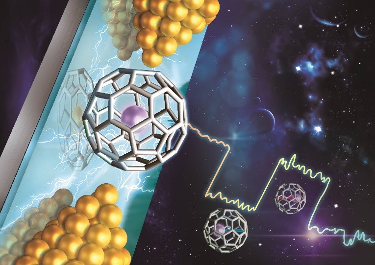
A Gd@C82 single-molecule electret
Electrets are a class of materials that can be compared to permanent magnets. They can be used for information storage, as well as for static earphones and microphones. It has long – lasting properties. The feature of electret was first discovered by Gray in 1732. In 1892, Heaviside combined electr-et (electret) with the phrase electric and magnet firstly, and clearly put forward the concept of electret5.

Fig.1 Single-electron transport of the Gd@C82 SMD

Fig.2 Density functional theory calculations revealing the SME physics
These two states probably correspond to two molecular configurations, but this configuration change is difficult to be directly observed by experiments, by using the first-principles calculation, it was found that Gd atom in the Gd@C82 molecule was located at the two most stable adjacent adsorption sites on the C82 cage, with an energy difference of ~ 6 meV (Fig. 2a). It can be seen that the positive and negative charge centers of Gd@C82 molecules do not coincide, that is, the molecule has a non-zero electric dipole moment.

Sliding ferroelectricity

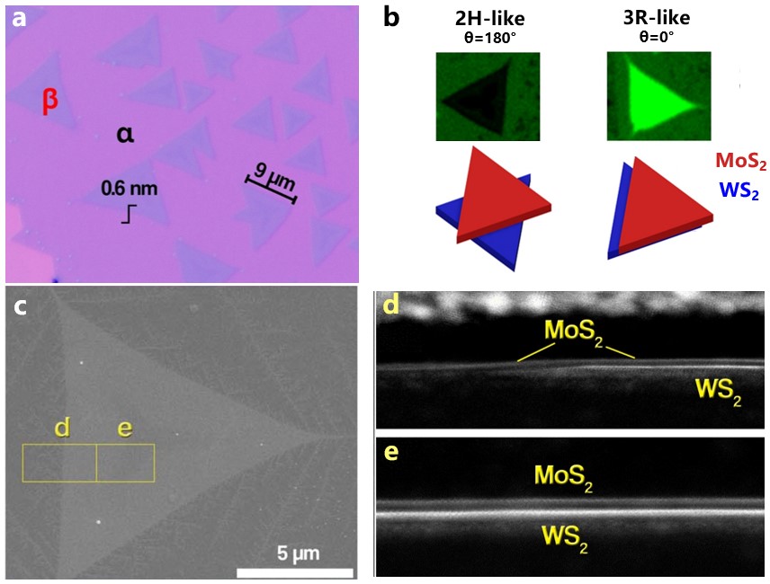
Fig.3 MoS2/WS2 heterobilayers grown by CVD method
Science
Ferroelectricity in Untwisted Heterobilayers of Transition Metal Dichalcogenides
Collaborators used chemical vapor deposition (CVD) to grow a untwisted MoS2/WS2 heterobilayers with a thickness of only about 1 nm. This heterobilayers has two stacking structures of 2H and 3R, both of which break the out-of-plane inversion symmetry(Fig.3). The PFM results show that the material has the out-of-plane ferroelectric property with the obvious ferroelectric hysteresis loops (Fig.4). The piezoelectric coefficient d33 is 1.95-2.09 pm/V. This value is about 6 times higher than that of monolayer α-In2Se3, which has the highest out-of-plane polarization among previously known 2D ferroelectric materials6.

Fig.4 Ferroelectric characterization of MoS2/WS2 heterobilayers

In addition, the ferroelectric thin film was constructed into a ferroelectric tunnelling junction(FTJ), shows an considerable on/off ratio(~103). By using the first-principles calculation. We had explored a reliable method to calculate the piezoelectric coefficient of 2D materials , and the calculated values of 2.28~2.40 pm/V are obtained, which are consistent with the experimental results. The calculation results show that the non-zero out-of-plane polarization comes from the interlayer charge transfer (Fig.5), and under the external electric field, the direction of interlayer charge transfer can be flipped by overcoming the 16 meV/f.u energy barrier, so that the polarization direction can be reversed through the in-plane sliding, indicating that the heterobilayers is an out-of-plane ferroelectric thin film.
1.https://www.electronics-tutorials.ws/electromagnetism/magnetic-hysteresis.html
