No Results Found
The page you requested could not be found. Try refining your search, or use the navigation above to locate the post.

Chinese Physics B
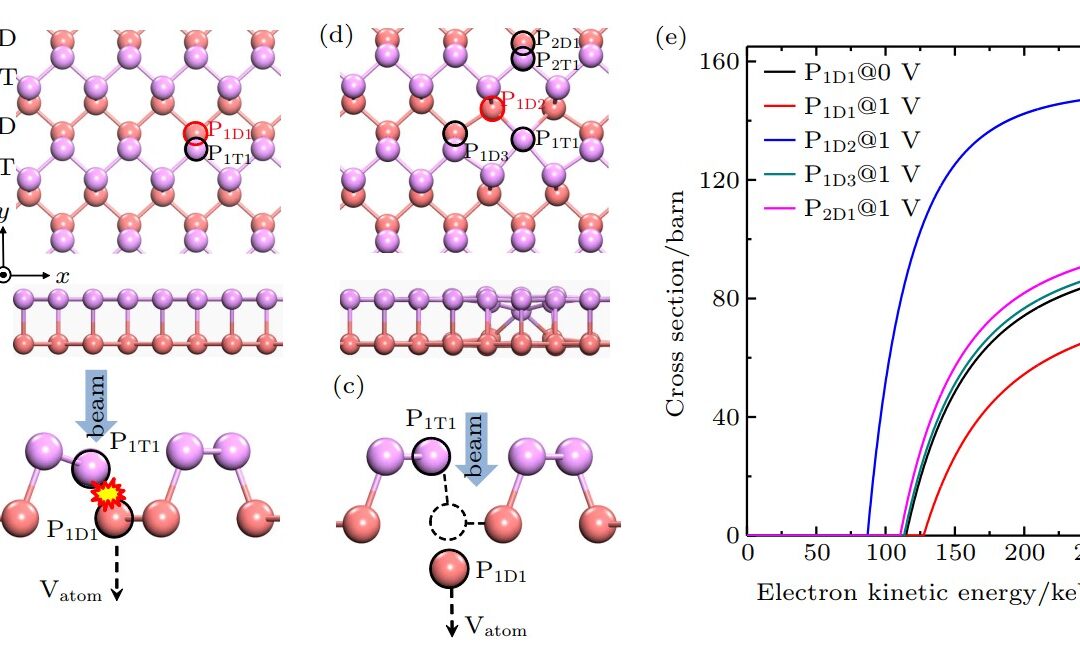
Fig.4 (a) Top and side views of atomic structure of monolayer BP (V0P). The names of the zigzag-like chains and two tested atoms are marked. The upper (colored in plum) and lower (colored in light coral) chains are named nT (n is the order number of the chain) and nD, respectively. The P atoms in the upper and lower sublayers are named PnTm (m is the order number of the atom) and PnDm, respectively. (b) and (c) Trajectories of two tested P atoms in pristine monolayer BP under an FHEEB. (d) Top and side views of the atomic structure of a single-atom vacancy BP (V1P) and all five tested P atoms. (e) Calculated cross-sections for the tested atoms in pristine monolayer BP (V0P) and single-atom vacancy monolayer BP (V1P).

Fig.5 Electrical properties of predicted zigzag chain vacancy in monolayer BP. (a) Band structure and density of states of the chain vacancy. (b) PCD at bands MB1 and MB2, DCD, and atomic structure of the zigzag edge chain. (c) Band structure of double-periodic chain vacancies with and without up-and-down distortion. (c) PCD at bands MB1 and MB2, DCD, and atomic structure of the zigzag edge chain. (d) Top view (left) and side view (right) of the atomic structure of the chain vacancy with distortion.
This simulation was implemented using a self-developed tool aBEST (https://gitee.com/jigroupruc/aBEST). This work is expected to inspire further works that will implement more exciton modeling methods into the simulation protocol and thus provide detailed theoretical guidance for future experiments in the field of 2D material etching by FHEEBs.
1. Zhao, X.; Loh, K. P.; Pennycook, S. J. Electron Beam Triggered Single-Atom Dynamics in Two-Dimensional Materials. J. Phys.: Condens. Matter 2020, 33 (6), 063001. https://doi.org/10.1088/1361-648X/abbdb9.
2. Molecular Beam Epitaxy of Highly Crystalline MoSe2 on Hexagonal Boron Nitride | ACS Nano, https://pubs.acs.org/doi/full/10.1021/acsnano.8b04037.
3. X. Zhao, Y. Ji, J. Chen, W. Fu, J. Dan, Y. Liu, S. J. Pennycook, W. Zhou, and K. P. Loh, Healing of Planar Defects in 2D Materials via Grain Boundary Sliding, Advanced Materials 31, 1900237 (2019).
4. Atomic Structure and Formation Mechanism of Sub-Nanometer Pores in 2D Monolayer MoS 2 – Nanoscale (RSC Publishing) DOI:10.1039/C7NR01127J, https://pubs.rsc.org/en/content/articlehtml/2017/nr/c7nr01127j.
5. O. Dyck, S. Kim, E. Jimenez-Izal, A. N. Alexandrova, S. V. Kalinin, and S. Jesse, Building Structures Atom by Atom via Electron Beam Manipulation, Small 14, 1801771 (2018).
6. Electron-Beam Manipulation of Silicon Dopants in Graphene | Nano Letters, https://pubs.acs.org/doi/full/10.1021/acs.nanolett.8b02406.
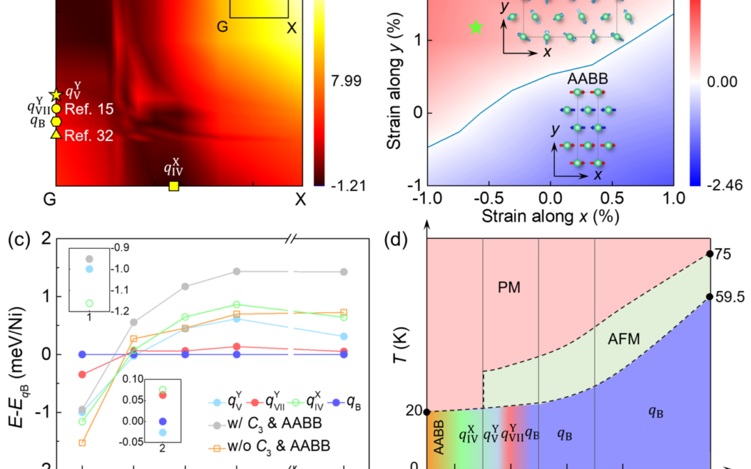

Fig.4 Layer-dependent magnetic groundstate of NiI2
Arxiv
Bulk NiI2 undergoes two successive magnetic phase transitions from a para-magnetic (PM) phase to an interlayer antiferromagnetic (AFM) phase at TN1 = 76 K and then to a spiral magnetic phase below TN2 = 59.5 K [12]. The AFM-to-spiral transition is accompanied by both rotational symmetry and inversion symmetry breaks, resulting in electric polarization through inverse DM interaction, as reflected in second harmonic generation (SHG) [13] and birefringence signals [14]
The monolayer (ML) of NiI2 was recently suggested to be a type-II multiferroic material, based on a presumed magnetic configuration and a supposed origin of the enhanced SHG signal. We found that such an assumption is flawed at the monolayer limit where a freestanding ML NiI2 showing broken C3 symmetry prefers to a striped antiferromagnetic order (AABB-AFM) along with an intralayer antiferroelectric (AFE) order[15]. However, the C3 symmetry of the monolayer may preserve under a substrate confinement, which leads to a spiral magnetic order (Spiral-V), a different spiral order from that of the bulk counterpart (Spiral-B). The Spiral-V order persists up to 2L thickness with the C3 symmetry and shows ferroelectricity (FE) ascribed to the inversed DM interaction. Thus, those three type-II multiferroic phases, namely Spiral-B+FE, Spiral-V+FE and AABB-AFM+AFE, emerge for NiI2 with different layer numbers and structural symmetries.
1. N. A. Spaldin and R. Ramesh, Nat. Mater. 18, 203 (2019)
2. H. Schmid, Ferroelectrics 162, 317 (1994)
3. M. Fiebig, T. Lottermoser, D. Meier, and M. Trassin, Nat. Rev. Mater. 1, 16046 (2016)
4. J. Wang, H. Z. J. B. Neaton, V. Nagarajan, S. B. Ogale, B. Liu, D. Viehland, V. Vaithyanathan, D. G. Schlom, U. V. Waghmare,, and K. M. R. N. A. Spaldin, M. Wuttig and R. Ramesh, Science 299, 1719
5. F. Zeng, G. Fan, M. Hao, Y. Wang, Y. Wen, X. Chen, J. Zhang, and W. Lu, J Alloy Compd 831, 154853 (2020)
6. D. L. Fox and J. F. Scott, Journal of Physics C: Solid State Physics 10, L329 (1977)
7. A. Prikockytė, D. Bilc, P. Hermet, C. Dubourdieu, and P. Ghosez, Phys. Rev. B 84 (2011)
8. B. B. Van Aken, T. T. Palstra, A. Filippetti, and N. A. Spaldin, Nat Mater 3, 164 (2004)
9. M. Lilienblum, T. Lottermoser, S. Manz, S. M. Selbach, A. Cano, and M. Fiebig, Nature Physics 11, 1070 (2015)
10. N. Ikeda, H. Ohsumi, K. Ohwada, K. Ishii, T. Inami, K. Kakurai, Y. Murakami, K. Yoshii, S. Mori, Y. Horibe et al., Nature 436, 1136 (2005)
11. R. E. Newnham, J. J. Kramer, W. A. Schulze, and L. E. Cross, Journal of Applied Physics 49, 6088 (1978)
12. T. Kurumaji, S. Seki, S. Ishiwata, H. Murakawa, Y. Kaneko, and Y. Tokura, Phys. Rev. B 87, 014429 (2013)
13. H. Ju, Y. Lee, K.-T. Kim, I. H. Choi, C. J. Roh, S. Son, P. Park, J. H. Kim, T. S. Jung, J. H. Kim et al., Nano Lett. 21, 5126 (2021)
14. Q. Song, C. A. Occhialini, E. Ergecen, B. Ilyas, D. Amoroso, P. Barone, J. Kapeghian, K. Watanabe, T. Taniguchi, A. S. Botana et al., Nature 602, 601 (2022)
15. N. Liu, C. Wang, C. Yan, C. Xu, J. Hu, Y. Zhang, and W. Ji, arXiv:2211.14423 (2022)


Nature Nanotechnology
Electrets are a class of materials that can be compared to permanent magnets. They can be used for information storage, as well as for static earphones and microphones. It has long – lasting properties. The feature of electret was first discovered by Gray in 1732. In 1892, Heaviside combined electr-et (electret) with the phrase electric and magnet firstly, and clearly put forward the concept of electret5.

Fig.1 Single-electron transport of the Gd@C82 SMD

Fig.2 Density functional theory calculations revealing the SME physics
These two states probably correspond to two molecular configurations, but this configuration change is difficult to be directly observed by experiments, by using the first-principles calculation, it was found that Gd atom in the Gd@C82 molecule was located at the two most stable adjacent adsorption sites on the C82 cage, with an energy difference of ~ 6 meV (Fig. 2a). It can be seen that the positive and negative charge centers of Gd@C82 molecules do not coincide, that is, the molecule has a non-zero electric dipole moment.


Fig.3 MoS2/WS2 heterobilayers grown by CVD method
Science
Collaborators used chemical vapor deposition (CVD) to grow a untwisted MoS2/WS2 heterobilayers with a thickness of only about 1 nm. This heterobilayers has two stacking structures of 2H and 3R, both of which break the out-of-plane inversion symmetry(Fig.3). The PFM results show that the material has the out-of-plane ferroelectric property with the obvious ferroelectric hysteresis loops (Fig.4). The piezoelectric coefficient d33 is 1.95-2.09 pm/V. This value is about 6 times higher than that of monolayer α-In2Se3, which has the highest out-of-plane polarization among previously known 2D ferroelectric materials6.

Fig.4 Ferroelectric characterization of MoS2/WS2 heterobilayers

In addition, the ferroelectric thin film was constructed into a ferroelectric tunnelling junction(FTJ), shows an considerable on/off ratio(~103). By using the first-principles calculation. We had explored a reliable method to calculate the piezoelectric coefficient of 2D materials , and the calculated values of 2.28~2.40 pm/V are obtained, which are consistent with the experimental results. The calculation results show that the non-zero out-of-plane polarization comes from the interlayer charge transfer (Fig.5), and under the external electric field, the direction of interlayer charge transfer can be flipped by overcoming the 16 meV/f.u energy barrier, so that the polarization direction can be reversed through the in-plane sliding, indicating that the heterobilayers is an out-of-plane ferroelectric thin film.
1.https://www.electronics-tutorials.ws/electromagnetism/magnetic-hysteresis.html

Two-dimensional magnetic materials with magnetic anisotropy can form magnetic order under limited temperature in the single-layer limit. Their macroscopic magnetism is closely related to the number of layers and stacking orders, and their magnetic exchange can be regulated by various external fields. These novel properties have endowed 2D magnetic materials with rich physical connotation and potential application value, which has attracted wide attention of researchers1.

Currently, two-dimensional magnetic materials reported in experiments mainly include transition metal halides, transition metal sulfides, transition metal carbonitides, transition metal phosphorus sulfides, Mn-Bi-Te family, etc. When the system degree is reduced to the single-layer limit, they usually exhibit significantly different magnetic behavior from that of bulk and less layered samples. These single-layer and few-layer magnetic materials are more easily regulated by external means, such as magnetic field, electric field, strain, light, etc. Therefore, the rich and highly adjustable magnetic phenomena of these two-dimensional magnetic materials indicate that they have broad development prospects in the application of two-dimensional devices.
Although a considerable number of intrinsic two-dimensional magnetic materials have been discovered, the related research on them is still in its infancy. The discovery of new mechanisms of magnetic coupling and magnetic regulation of two-dimensional magnetic materials and the design of intrinsic two-dimensional magnetic materials with high magnetic ordered transition temperatures are still challenging frontier scientific issues.
The page you requested could not be found. Try refining your search, or use the navigation above to locate the post.
Ji Group@Renmin University