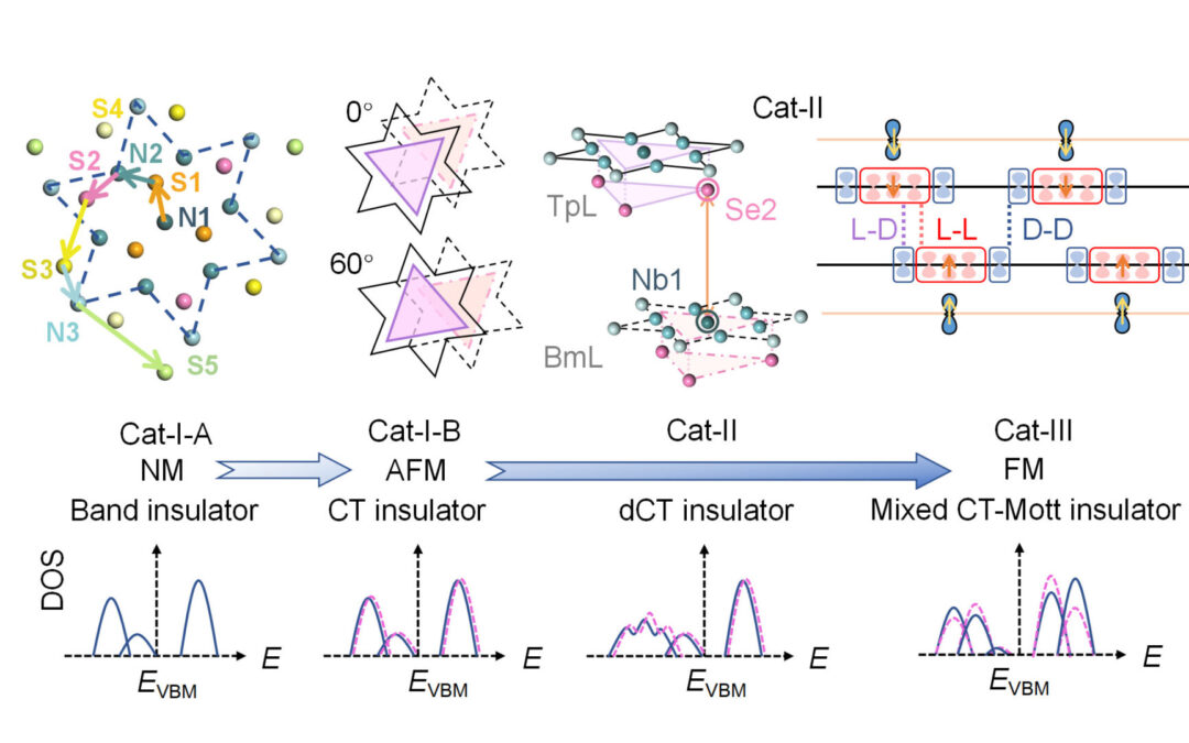
NbSe2

NbSe2

Arxiv

Layer sliding and twisting induced electronic transitions in correlated magnetic 1T-NbSe2 bilayers

Mott and CT insulators are representative materials, like 1T-phases of TaS2, TaSe2 and NbSe2. In the strong-correlation limit of electron correlated systems, on-site Coulomb interactions split a half-filled band into two sub-bands, namely the lower (LHB) and upper Hubbard bands (UHB), forming a Mott or a CT insulator[13]. The governing coupling mechanism lies in the interlayer electronic hybridization of interfacial Se pz orbitals within a localized region of the David star, rather than previously supposed metal atoms dz2 orbitals. Subtle differences in interlayer hybridization vary the energy levels of the four Hubbard bands in the 1T-NbSe2 bilayer. Three electronic and two magnetic transitions among four insulating states were observed upon interlayer sliding or twisting, while three of the four insulating states are correlated ones. All these striking results highlight the importance of interlayer coupling in tunning correlated electronic states in NbSe2 bilayers.

Mirror twin boundaries (MTBs)[14,15] was demonstrate to be another strategy to introduce additional exotic electronic states in chalcogen-deficient 1H-MoS2[16], -MoSe2[14], and – MoTe2[17]monolayers. In some lattices with specific symmetries, such as kagome lattice, the intrinsic flat band leads to a high density of electron states. A TMD layer consisting of ordered and uniformly sized MTB triangles, namely an MTB-triangle lattice, could be a TMD phase exhibiting a well-defined lattice symmetry. Coloring-triangular (CT) lattice[18] in a MoTe2 (CT-MoTe2) monolayer comprise of uniform-sized and orderly arranged MTB triangles and normal MoTe2 domains embedded among MTBs. Dirac-like and flat electronic bands inherently existing in the CT lattice are identified by two broad and two prominent peaks. Further more, the CT-MoTe2 monolayer shows energy-dependent electronic Janus lattices, including the original atomic-lattice and an electronic Te pseudo-sublattice.

REFERENCES

1. Zhang H, et al. Tailored Ising superconductivity in intercalated bulk NbSe2. Nature Physics 18, 1425-1430 (2022).

2. Cao Y, et al. Unconventional superconductivity in magic-angle graphene superlattices. Nature 556, 43-50 (2018)

3. Klanjšek M, et al. A high-temperature quantum spin liquid with polaron spins. Nature Physics 13, 1130-1134 (2017)

4. Law KT, Lee PA. 1T-TaS2 as a quantum spin liquid. Proceedings of the National Academy of Sciences 114, 6996-7000 (2017)

5. Chen Y, et al. Strong correlations and orbital texture in single-layer 1T-TaSe2. Nature Physics 16, 218-224 (2020)

6. Liu M, et al. Monolayer 1T-NbSe2 as a 2D-correlated magnetic insulator. Science Advances 7, eabi6339 (2021)

7. Wang YD, et al. Band insulator to Mott insulator transition in 1T-TaS2. Nature Communications 11, 4215 (2020)

8. Grasset R, et al. Pressure-induced collapse of the charge density wave and Higgs mode visibility in 2H− TaS2. Physical Review Letters 122, 127001 (2019)

9. Lian C-S, Si C, Duan W. Unveiling Charge-Density Wave, Superconductivity, and Their Competitive Nature in Two-Dimensional NbSe2. Nano Letters 18, 2924-2929 (2018)

10. Li H, et al. Imaging two-dimensional generalized Wigner crystals. Nature 597, 650-654 (2021)

11. Regan EC, et al. Mott and generalized Wigner crystal states in WSe2/WS2 moiré superlattices. Nature 579, 359-363 (2020)

12. Zhou Y, et al. Bilayer Wigner crystals in a transition metal dichalcogenide heterostructure. Nature 595, 48-52 (2021)

13. Zaanen J, Sawatzky GA, Allen JW. Band gaps and electronic structure of transition-metal compounds. Physical Review Letters 55, 418-421 (1985)

14. Liu H, et al. Dense Network of One-Dimensional Midgap Metallic Modes in Monolayer MoSe2 and Their Spatial Undulations. Physical Review Letters 113, 066105 (2014)

15. Hong J, et al. Inversion Domain Boundary Induced Stacking and Bandstructure Diversity in Bilayer MoSe2. Nano Letters 17, 6653-6660 (2017)

16. Zhou W, et al. Intrinsic Structural Defects in Monolayer Molybdenum Disulfide. Nano Letters 13, 2615-2622 (2013)

17. Diaz HC, Ma Y, Chaghi R, Batzill M. High density of (pseudo) periodic twin-grain boundaries in molecular beam epitaxy-grown van der Waals heterostructure: MoTe2/MoS2. Applied Physics Letters 108, 191606 (2016)

18. Zhang S, et al. Kagome bands disguised in a coloring-triangle lattice. Physical Review B 99, 100404 (2019)

AuTeSe

AuTeSe

Fig.1 Intercube Te-Te quasibonds and two interweaved charge orders in the ATS superatomic crystal

.

Physical review X

Interweaving Polar Charge Orders in a Layered Metallic Super-atomic Crysta

A superatom is any cluster of atoms that collectively exhibits some properties of single atoms. When arranged into crystals through the noncovalent bonds, they can be readily assembled into nanostructures, because the reduced cohesive energy of the noncovalent bonds makes it easier to cleave the material. It is not yet clear whether such weakened energetic interaction is accompanied by a suppressed electronic interaction among the superatoms. To that end, we explore exotic electronic structures on the surface of one superatomic crystal and find strong electron-electron interactions do occur. We also find that two exotic charge orders emerge.

Recently, researchers synthesized a cubic superatom, Au6Te12Se8 (ATS), and assembled it into a 3D crystal with metallicity and superconductivity.[9] In our experiments, we observe two charge orders on the ATS surface. One is a charge density wave that forms across repeating columns of ATS cubes. The other is a polar metallic state that arises between the columns. The polar metallic states are of particular interest, suggesting the ATS surface is an antipolar metal—a type of exotic metal where metallicity and orderly, antiparallel-oriented electric dipoles coexist. The discovery of this antipoloar metal goes one step further toward the realization of multifunctional devices, which could, in principle, perform simultaneous electrical, magnetic, and optical functions. However, we have not yet examined ATS’s ferroelectricity, which is needed for electrical control of its electrical polarization.

This ATS crystal is, to the best of our knowledge, the first antipolar metal ever found and possesses the first polar metallic state hosted in superatomic units bound by noncovalent interactions. Thus, the strong electron-electron interactions, found in the 2D superatomic layers, open a category of quantum materials that contains versatile layered nanostructures exhibiting precisely tailorable electronic structures.

REFERENCES

1. Z. Luo, A.W. Castleman, Special and General Superatoms, Accounts of Chemical Research 47 (2014) 2931-2940

2. Superatoms: Electronic and Geometric Effects on Reactivity, (2017)

3. E.A. Doud, A. Voevodin, T.J. Hochuli, A.M. Champsaur, C. Nuckolls, X. Roy, Superatoms in materials science, Nature Reviews Materials 5 (2020) 371-387

4. J. Puru, S. Qiang, Super Atomic Clusters: Design Rules and Potential for Building Blocks of Materials, Chemical Reviews 118 (2018) acs.chemrev.7b00524-

5. Z. Liu, X. Wang, J. Cai, H. Zhu, Room-Temperature Ordered Spin Structures in Cluster-Assembled Single V@Si12 Sheets, The Journal of Physical Chemistry C (2014)

6. E. Meirzadeh, A.M. Evans, M. Rezaee, M. Milich, C.J. Dionne, T.P. Darlington, S.T. Bao, A.K. Bartholomew, T. Handa, D.J. Rizzo, R.A. Wiscons, M. Reza, A. Zangiabadi, N. Fardian-Melamed, A.C. Crowther, P.J. Schuck, D.N. Basov, X. Zhu, A. Giri, P.E. Hopkins, P. Kim, M.L. Steigerwald, J. Yang, C. Nuckolls, X. Roy, A few-layer covalent network of fullerenes, Nature 613 (2023) 71-76

7. Evan, S., O’Brien, M., Tuan, Trin, Rose, L., Kann, Jia, Single-crystal-to-single-crystal intercalation of a low-bandgap superatomic crystal, Nature Chemistry (2017)

8. H. Yang, W. Yu, H. Huang, L. Gell, L. Lehtovaara, S. Malola, H. Hkkinen, N. Zheng, All-thiol-stabilized Ag44 and Au12Ag32 nanoparticles with single-crystal structures, Nature Publishing Group (2013)

9. Guo, J.G., Chen, X., Jia, X.Y. et al. Quasi-two-dimensional superconductivity from dimerization of atomically ordered AuTe2Se4/3 cubes. Nat Commun 8, 871 (2017)

Phase Patterning in 2D Materials

Phase Patterning in 2D Materials

Fig.1 a) The scheme of 2D ReS2 phase transition under STEM. a,b and a + b are the three low index directions of ReS2. e– beam exposure creates a new T phase embedded in the pristine T′ phase. b–d) Atomic structures and electronic structures of T’’ (tetramerization in two directions) phase, T’ (dimerization in one direction) phase, and T (no dimerization) phase from DFT calculation, respectively.

Advanced science

Sub-Nanometer Electron Beam Phase Patterning in 2D Materials

Fig.2 STEM HAADF images of atomic-scale phase transition from pristine T’’ phase into 1D T’ or T phases, via 1D e– beam exposure direction along a, b and a+b crystal directions (scheme on the right), respectively. False color is applied to STEM images. e– beam scanning areas are marked by green and red boxes. Scale bars =1 nm.

Fig.3 c) Energy-Surface Area (E-S) relations of T, T’ and T’’ phase under the uniaxial strain along a crystal direction. Different phases are shown by different symbols: T phase, green squares; T’ phase, orange dots; T’’ phase, blue triangles. d) E-S relations of T, T’, and T’’ phase under biaxial strain. Tangent lines are presented by the gray dotted lines.

Our DFT calculations reveal the energy-surface (E-S) relations of the three phases in 1L ReS2 under strain (Fig.3 c,d). In terms of the uniaxial case, the stability superiority of the T’’ phase reduces upon a compressive strain along lattice direction a and a crossover of the total energies of T’’and T’ phases is found. Yet the T phase remains very unstable under uniaxial compressive strain, and it becomes the most stable phase when a biaxial strain is applied. The transition lattice constants are comparable with the experimentally derived lattice constants measured. Formation energies of S vacancies (single and bi- vacancies) and their associated displacement threshold energies (Td) of 1L ReS2 were revealed by DFT calculations. It indicates S-3 vacancy is the easiest one to be created, which is consistent with the experimental observation.

This work demonstrates that down to atomic precision, the focused e– beam patterning technique is capable of engineering the metallic T or T’ phase from 1D line to 2D surface at both grain domains and boundaries on the semiconducting T’’ phased ReS2 and ReSe2 monolayers. It provides an ideal patterning precision up to the sub-Å scale after aberration correction and results in phase patterning areas from several to ≈100 nm2, which is orders of magnitude greater than any conventional lithography techniques.

Selective linear etching

Selective linear etching

Chinese Physics B

Selective linear etching of monolayer black phosphorus using electron beams

Fig.4 (a) Top and side views of atomic structure of monolayer BP (V0P). The names of the zigzag-like chains and two tested atoms are marked. The upper (colored in plum) and lower (colored in light coral) chains are named nT (n is the order number of the chain) and nD, respectively. The P atoms in the upper and lower sublayers are named PnTm (m is the order number of the atom) and PnDm, respectively. (b) and (c) Trajectories of two tested P atoms in pristine monolayer BP under an FHEEB. (d) Top and side views of the atomic structure of a single-atom vacancy BP (V1P) and all five tested P atoms. (e) Calculated cross-sections for the tested atoms in pristine monolayer BP (V0P) and single-atom vacancy monolayer BP (V1P).

Fig.5 Electrical properties of predicted zigzag chain vacancy in monolayer BP. (a) Band structure and density of states of the chain vacancy. (b) PCD at bands MB1 and MB2, DCD, and atomic structure of the zigzag edge chain. (c) Band structure of double-periodic chain vacancies with and without up-and-down distortion. (c) PCD at bands MB1 and MB2, DCD, and atomic structure of the zigzag edge chain. (d) Top view (left) and side view (right) of the atomic structure of the chain vacancy with distortion.

A special zigzag chain vacancy (Fig 5d) in monolayer BP was predicted by using high-energy electron beams (FHEEBs) and knocking away P atoms one by one along a zigzag chain in the lower sublayers. The calculated electronic properties of the chain vacancy showed that there was quasi-bonding between the two edges of the vacancy (Fig 5b), and a CDW was also formed along the vacancy. Our findings help improve understanding of quasi-bonding in which covalent-like states can also be half-occupied. The chain vacancy was a dynamically stable but thermodynamically metastable state according to our comparison of the stabilities of five typical edges in monolayer BP. It was inspiring that the electron beam could create a dynamically mostly stable but thermodynamically metastable vacancy, which is difficult to obtain using conventional chemical synthesis methods but easier to achieve using an electron beam. This characteristic proves that an FHEEB can create a special environment for defect development.

This simulation was implemented using a self-developed tool aBEST (https://gitee.com/jigroupruc/aBEST). This work is expected to inspire further works that will implement more exciton modeling methods into the simulation protocol and thus provide detailed theoretical guidance for future experiments in the field of 2D material etching by FHEEBs.

REFERENCES

1. Zhao, X.; Loh, K. P.; Pennycook, S. J. Electron Beam Triggered Single-Atom Dynamics in Two-Dimensional Materials. J. Phys.: Condens. Matter 2020, 33 (6), 063001. https://doi.org/10.1088/1361-648X/abbdb9.

2. Molecular Beam Epitaxy of Highly Crystalline MoSe2 on Hexagonal Boron Nitride | ACS Nano, https://pubs.acs.org/doi/full/10.1021/acsnano.8b04037.

3. X. Zhao, Y. Ji, J. Chen, W. Fu, J. Dan, Y. Liu, S. J. Pennycook, W. Zhou, and K. P. Loh, Healing of Planar Defects in 2D Materials via Grain Boundary Sliding, Advanced Materials 31, 1900237 (2019).

4. Atomic Structure and Formation Mechanism of Sub-Nanometer Pores in 2D Monolayer MoS 2 – Nanoscale (RSC Publishing) DOI:10.1039/C7NR01127J, https://pubs.rsc.org/en/content/articlehtml/2017/nr/c7nr01127j.

5. O. Dyck, S. Kim, E. Jimenez-Izal, A. N. Alexandrova, S. V. Kalinin, and S. Jesse, Building Structures Atom by Atom via Electron Beam Manipulation, Small 14, 1801771 (2018).

6. Electron-Beam Manipulation of Silicon Dopants in Graphene | Nano Letters, https://pubs.acs.org/doi/full/10.1021/acs.nanolett.8b02406.

Multiferroicity in NiI2

Multiferroicity in NiI2

Fig.4 Layer-dependent magnetic groundstate of NiI2

Arxiv

Varied competition among three multiferroic phases of NiI2 from the bulk to the monolayer limit

Bulk NiI2 undergoes two successive magnetic phase transitions from a para-magnetic (PM) phase to an interlayer antiferromagnetic (AFM) phase at TN1 = 76 K and then to a spiral magnetic phase below TN2 = 59.5 K [12]. The AFM-to-spiral transition is accompanied by both rotational symmetry and inversion symmetry breaks, resulting in electric polarization through inverse DM interaction, as reflected in second harmonic generation (SHG) [13] and birefringence signals [14]

The monolayer (ML) of NiI2 was recently suggested to be a type-II multiferroic material, based on a presumed magnetic configuration and a supposed origin of the enhanced SHG signal. We found that such an assumption is flawed at the monolayer limit where a freestanding ML NiI2 showing broken C3 symmetry prefers to a striped antiferromagnetic order (AABB-AFM) along with an intralayer antiferroelectric (AFE) order[15]. However, the C3 symmetry of the monolayer may preserve under a substrate confinement, which leads to a spiral magnetic order (Spiral-V), a different spiral order from that of the bulk counterpart (Spiral-B). The Spiral-V order persists up to 2L thickness with the C3 symmetry and shows ferroelectricity (FE) ascribed to the inversed DM interaction. Thus, those three type-II multiferroic phases, namely Spiral-B+FE, Spiral-V+FE and AABB-AFM+AFE, emerge for NiI2 with different layer numbers and structural symmetries.

REFERENCES

1. N. A. Spaldin and R. Ramesh, Nat. Mater. 18, 203 (2019)

2. H. Schmid, Ferroelectrics 162, 317 (1994)

3. M. Fiebig, T. Lottermoser, D. Meier, and M. Trassin, Nat. Rev. Mater. 1, 16046 (2016)

4. J. Wang, H. Z. J. B. Neaton, V. Nagarajan, S. B. Ogale, B. Liu, D. Viehland, V. Vaithyanathan, D. G. Schlom, U. V. Waghmare,, and K. M. R. N. A. Spaldin, M. Wuttig and R. Ramesh, Science 299, 1719

5. F. Zeng, G. Fan, M. Hao, Y. Wang, Y. Wen, X. Chen, J. Zhang, and W. Lu, J Alloy Compd 831, 154853 (2020)

6. D. L. Fox and J. F. Scott, Journal of Physics C: Solid State Physics 10, L329 (1977)

7. A. Prikockytė, D. Bilc, P. Hermet, C. Dubourdieu, and P. Ghosez, Phys. Rev. B 84 (2011)

8. B. B. Van Aken, T. T. Palstra, A. Filippetti, and N. A. Spaldin, Nat Mater 3, 164 (2004)

9. M. Lilienblum, T. Lottermoser, S. Manz, S. M. Selbach, A. Cano, and M. Fiebig, Nature Physics 11, 1070 (2015)

10. N. Ikeda, H. Ohsumi, K. Ohwada, K. Ishii, T. Inami, K. Kakurai, Y. Murakami, K. Yoshii, S. Mori, Y. Horibe et al., Nature 436, 1136 (2005)

11. R. E. Newnham, J. J. Kramer, W. A. Schulze, and L. E. Cross, Journal of Applied Physics 49, 6088 (1978)

12. T. Kurumaji, S. Seki, S. Ishiwata, H. Murakawa, Y. Kaneko, and Y. Tokura, Phys. Rev. B 87, 014429 (2013)

13. H. Ju, Y. Lee, K.-T. Kim, I. H. Choi, C. J. Roh, S. Son, P. Park, J. H. Kim, T. S. Jung, J. H. Kim et al., Nano Lett. 21, 5126 (2021)

14. Q. Song, C. A. Occhialini, E. Ergecen, B. Ilyas, D. Amoroso, P. Barone, J. Kapeghian, K. Watanabe, T. Taniguchi, A. S. Botana et al., Nature 602, 601 (2022)

15. N. Liu, C. Wang, C. Yan, C. Xu, J. Hu, Y. Zhang, and W. Ji, arXiv:2211.14423 (2022)